10+ timer block diagram
Carrier Block Diagram KU040 and KU060 DIO. The figure below shows a detailed block diagram of the timercounter.
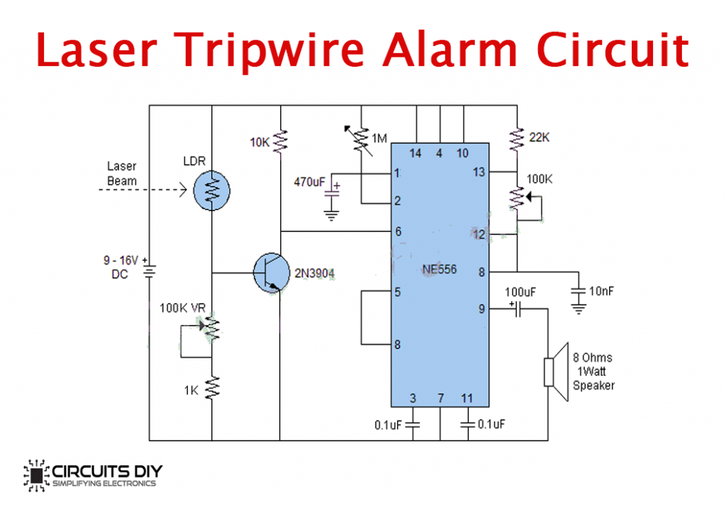
Top 10 Simple Electronics Projects For Complete Beginners
In order to determine the gain between an input or disturbance and any other points in the diagram it is necessary to identify two topological features of a block diagram.

. PMC Block Diagram Versal ACAP Technical Reference Manual AM011 Document ID AM011 Release. The block diagram representation of an ideal integrator is shown in Figure-1. Digital Clock Circuit Block Diagram Digital Clock Circuit Diagram To avoid blocking up space the alarm module is provided a separate digital clock circuit block diagram.
It is used to design new systems or to describe and improve existing ones. Circuit Diagram of Police Siren Circuit using NE555 Timer Components Required 555 Timer IC x 2 Resistors 1KΩ 10KΩ x 3 68KΩ Capacitors 100nF x 2 10µF x 2 Mini. The following figure shows a block diagram of the carrier portion of the PCIe-5785 KU040 and KU060 FPGA versions.
Webb ESE 499 3 Block Diagrams In the introductory section we saw examples of block diagrams to represent systems eg. Its structure provides a high-level overview. Figure 1shows the block diagram for the TIM1 timer peripheral.
TABLE 10-1 Block Diagram Reduction Rules 1 Combine all cascade blocks 2 Combine all parallel blocks 3 Eliminate all minor interior feedback loops 4 Shift summing points to left 5 Shift. Platform Management Controller Functional Block Diagram. Lecture 15 Block Diagram Design Examples Design Elements for Proof-of-Concept Top N Capability Functional Oriented Requirements State and Explain what your solution must.
The STM32 timer peripheral is made by the assembly of four units. HPS-FPGA Bridges Address Map and Register Definitions for Arria. The 8254 uses HMOS technology and comes in a 24-pin plastic or CERDIP package.
The following figure shows a block having input X s output Y s and the transfer function G s. Adder The adder is an element which is used to perform the addition and subtraction of the signals. Transfer Function G s Y s X s Y s G s X s Output of the block is obtained by.
The masterslave controller unit 2. The time-base unit 3. Functional Description of the HPS-FPGA Bridges 94.
Electronics Hub - Tech Reviews Guides How-to Latest Trends. The Counter TCAnCNT register Period and Compare TCAnPER and. Block diagrams consist of Blocks these represent.
The 8254 is a superset of the 8253. Arria 10 HPS-FPGA Bridges Block Diagram and System Integration 93. All modes are software programmable.
A block diagram is a specialized high-level flowchart used in engineering.
2

Atx Power Supply Pinout Diagram And Connector 20 24 Pin Etechnog

Hero Honda Wiring Diagram Http Bookingritzcarlton Info Hero Honda Wiring Diagram Motorcycle Wiring Electrical Wiring Diagram Electrical Diagram
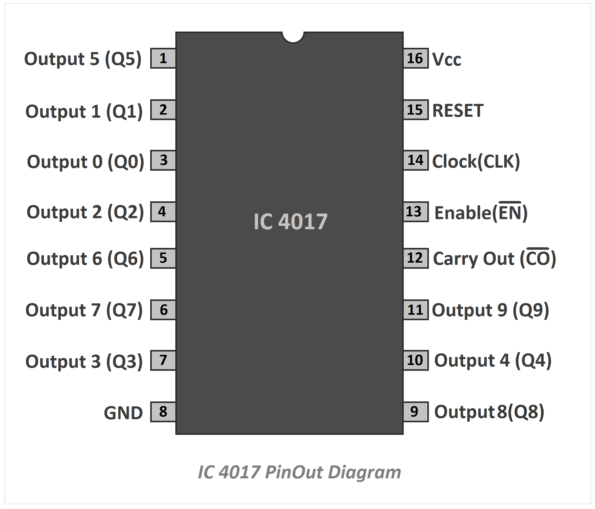
Ic 4017 Pinout Diagram And Terminal Identification Etechnog

Plc Programming Questions And Answers Programmable Logic Controller Plc Programming Electronic Engineering
Motorcycle Wiring Electrical Wiring Diagram Electrical Diagram

On Delay Timer Connection Diagram And Testing Etechnog

10 Online Ee Circuit Design Simulation Tools Software Electronic Engineering Circuit Design Simulation
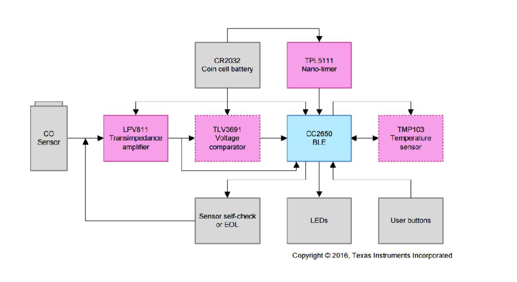
Always On Low Power Gas Sensing With 10 Year Coin Cell Battery Life Reference Design Electronics Lab Com
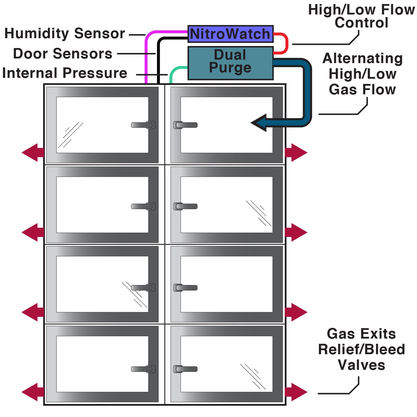
Isodry Nitrowatch Controller 9500 06a Terra Universal
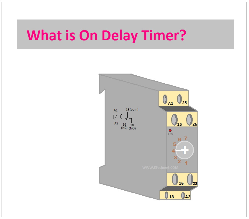
On Delay Timer Off Delay Timer On Off Delay Timer Etechnog

Digital Timer 30 Seconds Electronic Stopwatch Gradient Dial Starting Vector Icon Clock Watch Timer Countdown Symbol Vector Il Digital Timer Vector Illustration
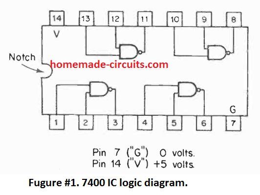
Simple Circuits Using Ic 7400 Nand Gates Homemade Circuit Projects

Motor Alarm Electronic Circuit Projects Electronics Projects Diy Electronics Circuit

Pin On Details Insulation Waterproofing

Idc Cable Breakout Board 10 Pin 2x5 0 1 Pmd Way

Arduino Uno Pinout Diagram And Pin Configuration Explained Etechnog